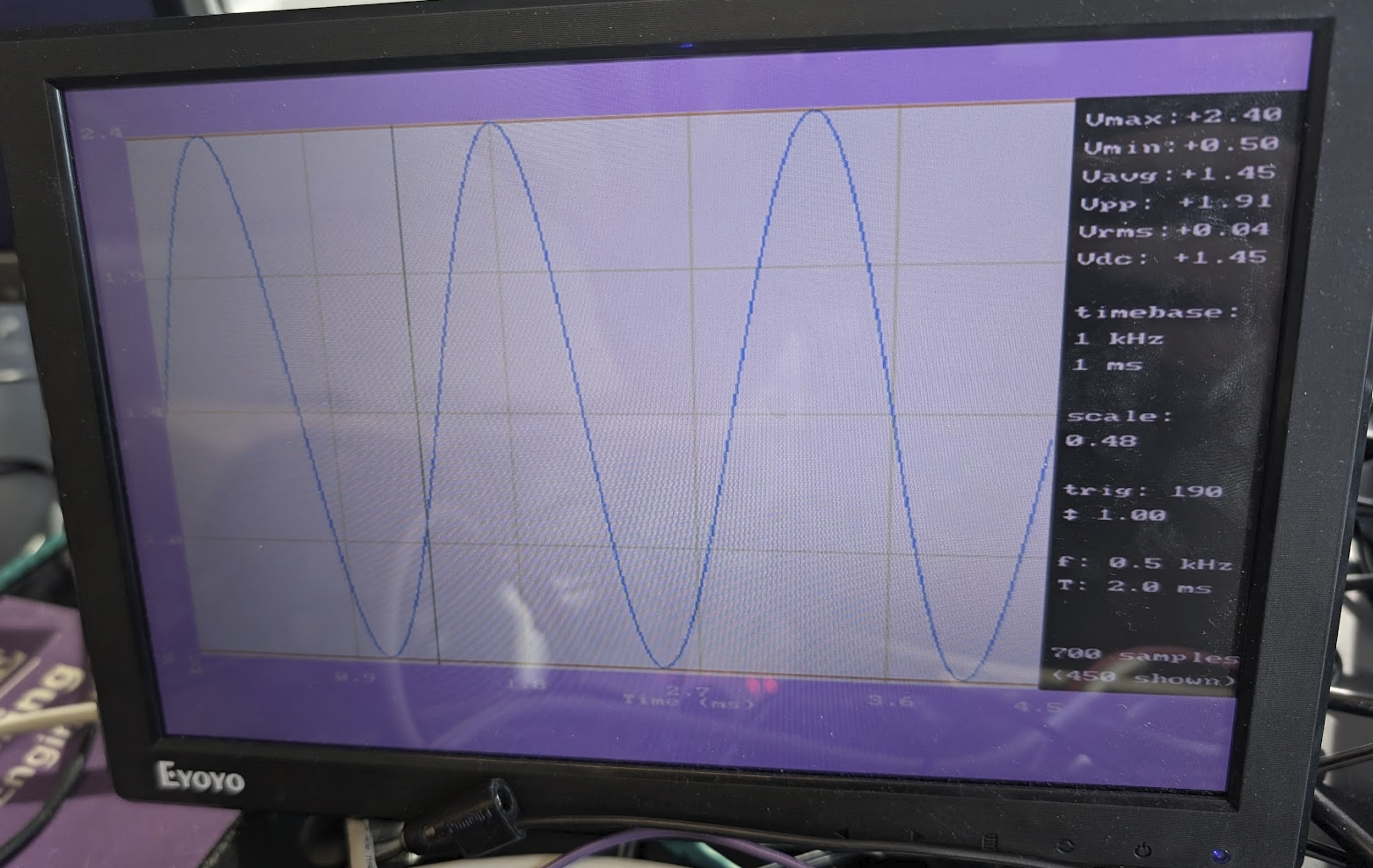
A Oscilloscope powered by an Intel Altera FPGA dev board created by Terasic. The FPGA samples singals from a ADC input and stores it in a buffer, which is read continuously or on trigger. The embedded Linux SoC runs a C program that reads this buffer, processes the data, and stores drawing instructions to another buffer. The FPGA reads this bugger to produce an output to a screen via VGA.
The program analyzes peak-to-peak, RMS, average, minimum, maximum, and DC offet voltages. The timebase and vertical scale are variable (zoom in/out) and can be determined automatically, which is displayed on the screen. A simple fourier analyisys shows the frequency and period of the signal. The graph displays the trigger point (rising/falling/edge/none) on the waveform, a background grid with labeled time/voltages, and the max/min lines. The waveform is automatically centered vertically, and the labels for the grid’s ticks are determined automatically.
Intel Quartus, and ModelSim were used for this, along with remote development tools like SSH.